1. OVERVIEW
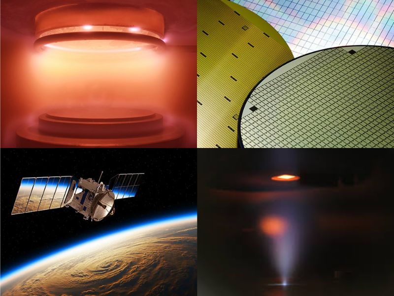
The development of thin films and their deposition methods have significantly contributed to the improvement of many industries over the past century. These industries include: Semiconductor, Magnetic recording material, Integrated circuits, LEDs, Optical coatings (such as anti-reflective coatings), Hard coatings for tool protection, Pharmaceuticals, Medicine, …
Thin film processing plays an important role in the research, development, and functionalization of surfaces. The application of this technology is very broad in the fields of: Microelectronics, Nanotechnology, Optoelectronics, Mechanics, Optics, Photonics, Textiles, Surface coating, Chemistry, Biology, Medicine
Thin Film Processing Techniques:
- Magnetron sputtering: A thin film deposition technique that bombards a metal cathode with ions generated in a magnetic field.
- ALD (Atomic Layer Deposition): A method of depositing atomic layer by layer, allowing control of film thickness at the atomic level.
- CVD (Chemical Vapor Deposition): A technique for depositing thin films from the gas phase, using chemical reactions between precursor gases.
- MOCVD (Metal Organic Chemical Vapor Deposition): A variant of CVD that uses metal organic compounds as precursors.
- PECVD (Plasma Enhanced Chemical Vapor Deposition): Plasma-assisted CVD, which improves the deposition rate and properties of the film.
- MBE (Molecular Beam Epitaxy): A technique for depositing epitaxial thin films from molecular beams.
- RIE (Reactive Ion Etching): A plasma etching technique that uses reactive ions to selectively etch materials.
- IBE/RIBE (Ion Beam Etch and Reactive Ion Beam Etch): A material etching technique using an ion beam or reactive ion beam.
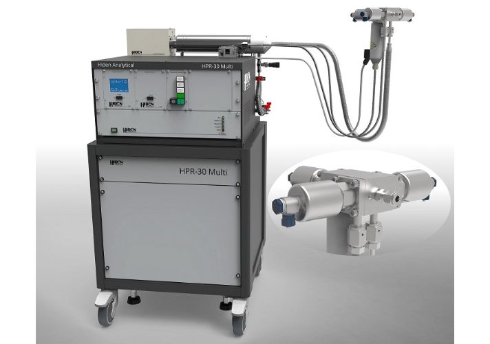
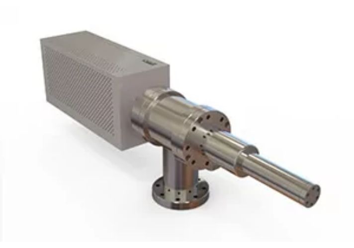
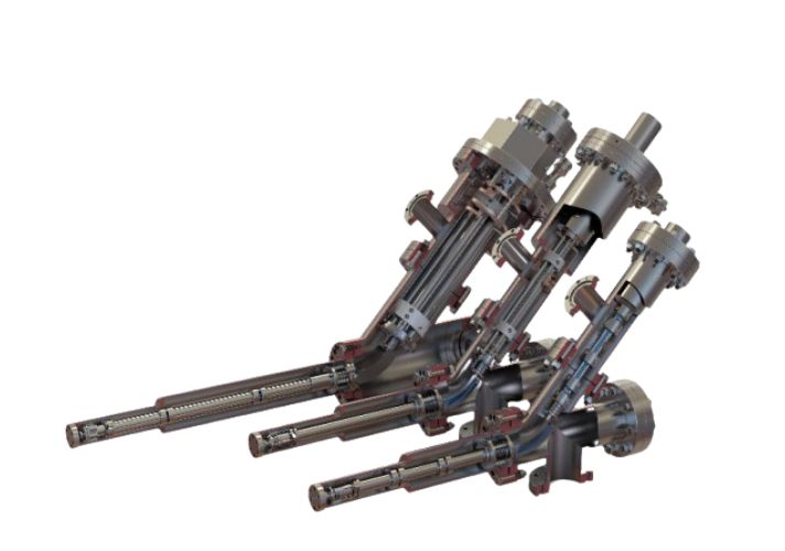
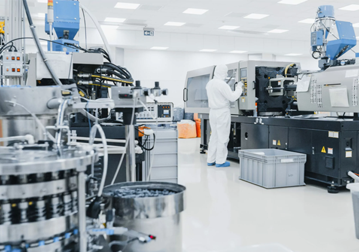
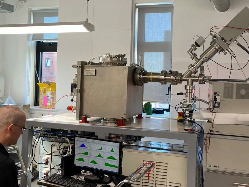
Each technique is typically used for a specific application, requiring specific process parameters to create the desired surface/film properties. Hiden Analytical quadrupole mass spectrometers provide insight into the processing and characterization of thin films, enabling optimization of thin film production and surface quality. Hiden systems are individually configured to ensure optimum sensitivity and speed in analysis.
2. APPLICATION
- Control of critical reaction components in optical thin film coating: Hiden Analytical mass spectrometries include industry-standard data interface options to enable integration of automatic production control. Hiden’s ultra-sensitive residual gas analyzers can detect moisture, hydrocarbons, and leaks, allowing for production monitoring. Hiden’s residual gas analyzer line includes systems for monitoring a variety of processing techniques, including evaporation, plasma, CVD, and magnetron sputtering.
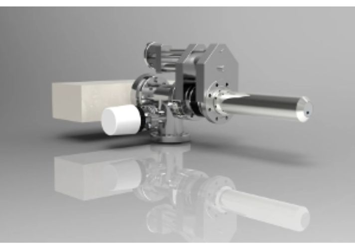
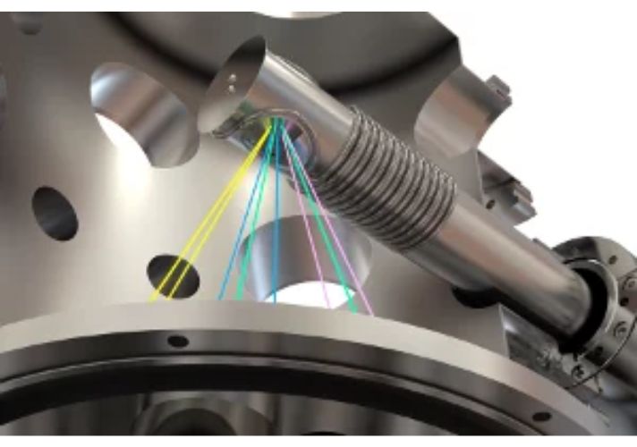
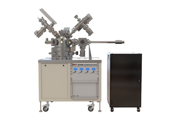
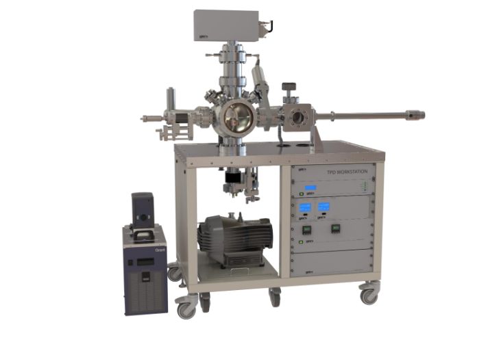
- Thin film and surface engineering: Hiden mass spectrometers are used for process control including SIMS endpoint detection of ion beam etching of magnetic thin films, III-V layers including gallium arsenide, and superconducting thin films including YBaCuO (yttrium barium copper oxide), and for flux monitoring when precise control of film growth is required in MBE (molecular beam epitaxy).
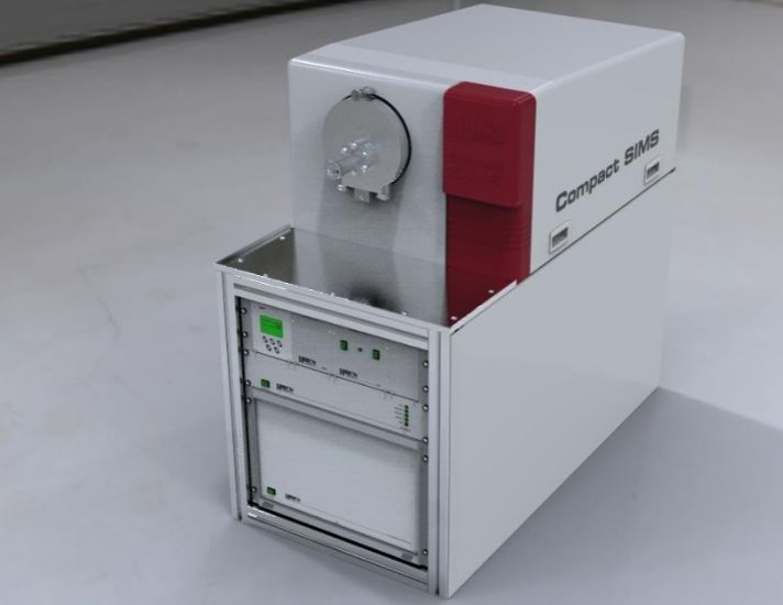
- UHV Surface Science: Polydimethylsiloxane (PDMS) is used as a lubricant in cosmetics, food additive [E900] and a sealant very popular in the industry. However, PDMS can decompose into silicon dioxide (glass), forming an insulating layer in electronic devices and making it difficult to bond surfaces, it is also very difficult to remove. Hiden Analytical’s SIMS equipment can easily detect the presence of this important industrial contaminant.
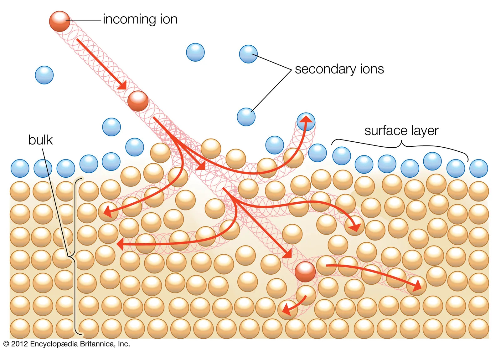
- FIB-SIMS for Nano-scale Materials Analysis: SIMS is critical for dopant analysis in semiconductor materials, applications in direct measurement of ion implantation dose and diffusion; measuring layer thickness, layer sharpness and alloy composition; and monitoring metallization, passivation and contamination processes.
- Plasma Deposition for Enhanced Surface Charateristics: Mass spectrometry contributes to the study of biocatalytic reaction kinetics by directly measuring the consumption and production of gases generated by enzymes through real-time high-sensitivity mass spectrometry.
- Plasma Etching & ALE (Atomic Layer Etching): In plasma processing, it is crucial to maintain optimal plasma conditions for the process. Atomic Layer Etching (ALE) is a two-step process that enables reliable, precise etching of one atomic layer at a time. The first step involves creating a reaction layer on the surface. The second step removes this layer and the underlying substrate in a self-limiting manner. For the second step to be self-limiting, it is important that the ion energy is higher than the sputtering threshold of the reaction layer but lower than that of the substrate. The radical and ion fluxes are also important for the formation of the reaction layer. Hiden PSM or EQP is used to monitor both the flux of radicals and ions and their energy in real time.
- Plasma Characterization Studies: Plasma-based technologies are used in many industrial processes, and new applications are rapidly developing. In the microelectronics industry, the need for higher throughput and smaller device sizes means that process and understanding are critical. Hiden plasma probes measure a number of key plasma parameters and provide insights into the plasma reaction chemistry.